
|
|
 |
|
Art's Parts
|
|
|
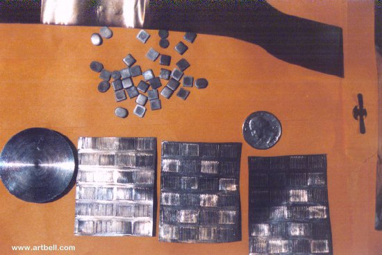
For those who have come into this late, please read the Anonymous Letters regarding this material first. Note: Additional photos and materials were not available for posting to the web site at this time, due to the amount of time it takes to process the photo images and transcribe the data. However, these are a good representative sampling of all the photos and graphs. The ones that are available are provided with a link. Click on the hyper-linked words and thumbnail images to see the full-sized view of the figures and photos. There are some real cool electron microscope images here. Preliminary Analyses of Art's Parts - 6/4/96Three types of specimens were received for analysis. We refer to them here as: 1) the "chips"; 2) the "metal strip"; and 3) the "vent". All of these have been presented earlier in a photograph on Art's Web Page. 1. The chips.
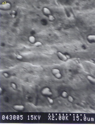
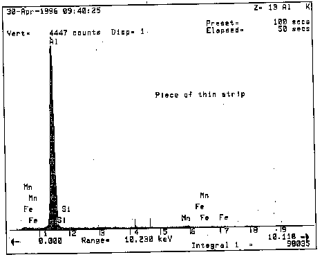
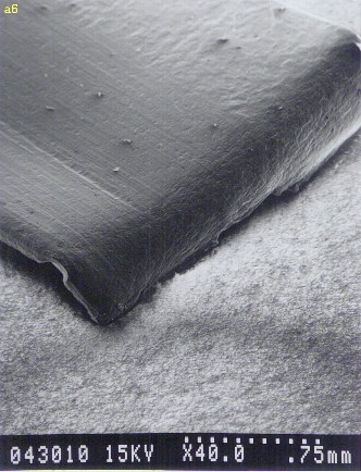
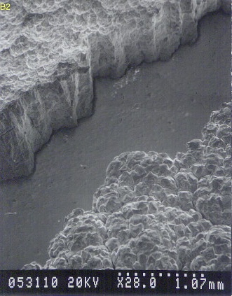
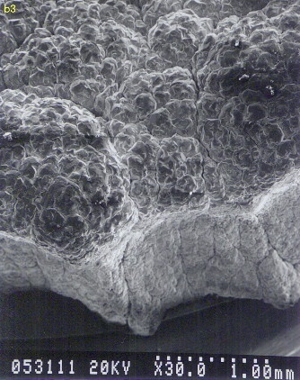
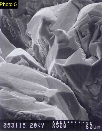
At this point, analyses have been conducted only on the square chips. Using a micrometer, a representative square chip had the dimensions: 6.368 mm x 6.361 mm x 1.596 mm. This gives a volume of 64.65 mm^3. Using a weight of 160 mg, this would correspond to a density of 2.47 mg/mm^3. The squares had two distinguishable sides: a "top" side with rounded edges, and a "bottom" side that was squared off --as if they had possibly been "punched out" from the top. Using a scanning electron microscope (SEM), photographs of the top side (photo 1) and the bottom side (photo 2) were generated. The SEM was configured for energy dispersive spectroscopy (EDS) which allows determination of the elemental content of the area being scanned by the electron beam. The bombardment of electrons results in the release of X-rays whose wavelengths are characteristic of the elements being targeted. A detector is able to translate this information into specific "peaks" which are then recorded. The analyses showed that over a broad (averaged) area on the surface of the top and bottom of the square chips (Figure 1 and Figure 2), only aluminum (Al) could be detected. It was also noted that despite the differences in apparent texture on the sides of the chips, the EDS spectra were essentially identical (not shown) -- i.e. only aluminum was detected in both the rougher and smoother portions. The density of aluminum is 2.7 and thus close to the value of 2.47 determined from our calculation. The curved top edges might contribute to the small difference. High magnification showed small granular particles embedded in the surface of the squares (photo 3 and photo 4). These had sizes of just a few microns (um). EDS showed that these contained silicon (Si) (Fig. 3). A square chip was embedded in epoxy, cut through the middle and polished in order to obtain a good cross section for SEM and EDS analyses. The SEM was done using a "backscattering" configuration which allows heavier elements to look brighter than less-heavy elements. Photo 5 shows that there are white (i.e. brighter) particulate flake-like materials scattered through the aluminum. These particles had a high iron (Fe) content as indicated in Fig.5 where the area measured was within a single particle. Small amounts of silicon (Si) and manganese (Mn) were also evident. The elements in these particles were not detectable when EDS was measured over a broad area of the chip cross-section (Fig. 4), presumably because of their small respective areas. 2. The metal strip.
3. The vent.
The slits are in 24 "groups" with 10 parallel slits one mm apart in each group. The lengths of the slits are 8 mm. When held up to the light at an angle, light can be seen through the parallel slits. The slits in each group appear oriented opposite to those in the adjacent group. That is, if considered to act in a vent-like manner, air going through the slits would be directed "up" in one group and "down" in the adjacent group. A small piece of the vent on one corner was removed for analysis. One edge of this piece corresponds to a slit edge. An SEM image is seen in photo 6. EDS showed it to consist primarily of aluminum (Fig. 8). This was similar for the three different sections that seemed to have a different textural appearance. Granules seen at high magnification exhibited the EDS pattern shown in Fig. 9. In this case the granules showed a content similar to the metal strip granules -- i.e. aluminum with small amounts of iron, manganese, calcium and silicon. Art's Parts -- The Skin(preliminary analyses)
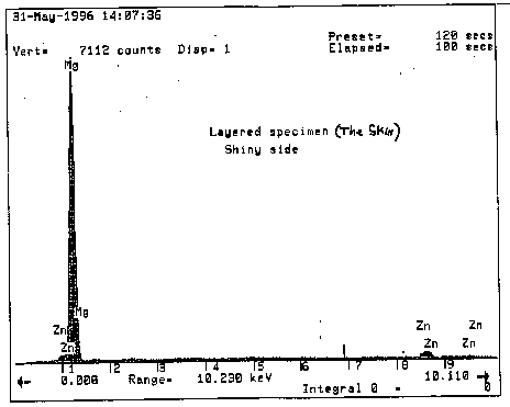
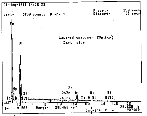
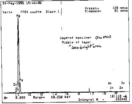
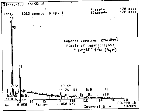
Each sapmle had a "silvery," shiny side with a rough (granular) appearance. The other side was blackish-gray. Looking at the samples edge-on, numerous layers can be seen. The samples were hard but brittle, and a few small pieces could be broken off using a small hand vice and manual pressure. Two such samples broken off were analyzed (side by side) by scanning electron microscopy (SEM); one was shiny side up-- the other was dark side up. Photo 2 shows a portion of both pieces; the shiny side up is in the lower right, while the dark side is in the upper left. Photo 3 shows the shiny side-up piece and includes a view of the edge where the layering can be noted. Photo 4 and photo 5 show higher magnifications of the shiny side. Energy dispersive spectroscopy (EDS) revealed the the shiny side contained more than 95% magnesium (Mg) and a small amount (2-3%) of zinc (Zn) (Fig. 1). The dark side contained a significant amount of bismuth (Bi) (Fig. 2). A small piece was embedded in epoxy, cut through, and polished in such a way that a cross section of the layering could be visualized. Photos 6,7, and 8 show images of the cross section at different magnifications. In these cases we utilized a backscattering mode which shows heavier elements to be brighter than less-heavy elements. As seen in the photos there are layers of lighter (less bright) material separated by much thinner layers of heavier (brighter) material. When EDS scans were done on the lighter material, a high level of magnesium was observed, again with a small amount of zinc (Fig. 3); whereas scans of the bright material showed a significant content of bismuth (Fig. 4). The thickness of the "bismuth layers" appear to be only a few microns. As seen in photo 6 and photo 7, there are apparent "bismuth layers" that appear less bright than others. Possibly this relates to a lower concentration of bismuth, or the bands occur slightly below the surface being examined. Additional studies will be necessary to determine which, if either, of these interpretations is correct. Thus the material appears to represent layers of a substance consisting mainly of magnesium and a small amount of zinc separated by thin layers containing a high bismuth content. END OF REPORT Transcribed by Keith & Mary Rowland from the original report received by Art Bell. Please do not copy this to other sites. Point all references here. |
 |
|
 |
|


![[IMAGE]](img/debrisa.jpg)
![[IMAGE]](img/debrisd.jpg)
![[IMAGE]](img/debrisc.jpg)
![[IMAGE]](img/skin1a.jpg)